
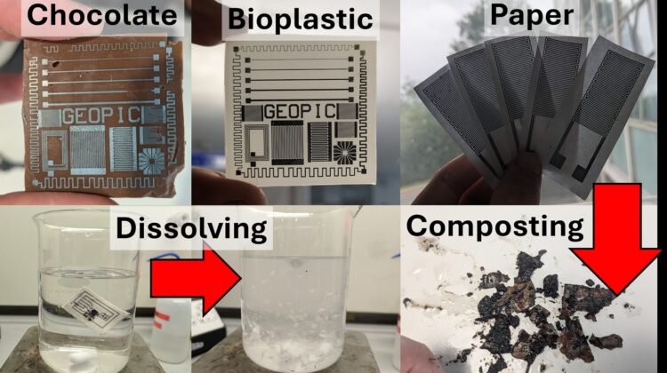
Researchers from the University of Glasgow have developed a new method of printing zinc-based electronic circuits on environmentally friendly surfaces including paper and bioplastics. Once the circuits are no longer needed, 99 per cent of their materials can be disposed of safely through ordinary soil composting or by dissolving in widely available chemicals, such as vinegar.
The research aims to address the growing problem of electronic waste, or e-waste, caused by the materials used in the construction of modern electronic devices. Conventional circuit boards are made from materials that are difficult or costly to recycle at the end of their lifecycle, and they often end up in landfill, where they can release harmful chemicals into the surrounding land. In 2024, 62 million tonnes of electronic waste were discarded, with less than 17 per cent recycled in the EU.
Advertisement

The team set out to help tackle the problem by developing what they call a ‘growth and transfer additive manufacturing process’, which generates conductive metal tracks on biodegradable surfaces.
Unlike conventional circuit boards, which use copper to conduct electricity, the team used zinc to create metal traces just five microns wide. The process works by electroplating conductive bulk zinc onto a temporary carrier, which is then transferred to a biodegradable base.
Advertisement

The resulting circuits perform comparably to traditional boards. The team tested them successfully in multiple devices, including tactile sensors, LED counters and temperature sensors. The team has also shown that the materials’ performance remains stable after more than a year when kept in ambient conditions.
A life cycle assessment conducted by the team compared the potential environmental impact of their new printed circuit boards (PCBs) against conventional boards. Their findings show that the biodegradable PCBs could enable a 79 per cent reduction in global warming potential, and a 90 per cent reduction in resource depletion, suggesting that they could enable significant reductions in the environmental impact of electronic devices.
Advertisement
‘The work demonstrates a major step toward circular electronics, where devices are designed from the outset for reuse, recycling, or safe degradation,’ said Jonathon Harwell of the University of Glasgow’s James Watt School of Engineering. ‘Discarded devices already generate tens of millions of tonnes of waste annually, so our research could have far-reaching impacts for consumer electronics, internet-of-things devices and disposable sensors in the future.’
‘One key aspect of our work is that almost any substrate material can be used in the process, ranging from paper and bioplastics for more realistic applications, to chocolate for tasty but probably not very practical demonstrations,’ said the James Watt School of Engineering’s Professor Jeff Kettle. ‘We are now exploring ways to adapt this technique to other fields, such as mouldable electronics or biosensing, which could also benefit from a cheap and versatile way to make high quality circuits with low environmental footprints.’
The research has been published in Communications Materials.
Advertisement