
A team of MIT engineers has designed a specially tailored treatment that makes the boiling of water and other liquids more efficient using a combination of three different kinds of surface modifications, each at different size scales.
The boiling of water or other fluids is an energy-intensive step at the heart of a wide range of industrial processes, including most electricity generating plants, many chemical production systems and even cooling systems for electronics. Improving the efficiency of the systems that heat and evaporate water could significantly reduce their energy use.
Advertisement

There are two key parameters that describe the boiling process: the heat transfer coefficient and the critical heat flux (CHF). In materials design, there’s generally a trade-off between the two, so anything that improves one of the parameters tends to make the other worse. But both are important for the efficiency of the system, and now, after years of work, the team has achieved a way of significantly improving both properties at the same time by adding a combination of different textures to a material’s surface.
‘Both parameters are important,’ said recent MIT graduate Youngsup Song, ‘but enhancing both parameters together is kind of tricky because they have intrinsic trade off.’ The reason for that, he explained, is ‘because if we have lots of bubbles on the boiling surface, that means boiling is very efficient, but if we have too many bubbles on the surface, they can coalesce together, which can form a vapour film over the boiling surface.’ That film introduces resistance to the heat transfer from the hot surface to the water. ‘If we have vapour in between the surface and water, that prevents the heat transfer efficiency and lowers the CHF value.’
Advertisement

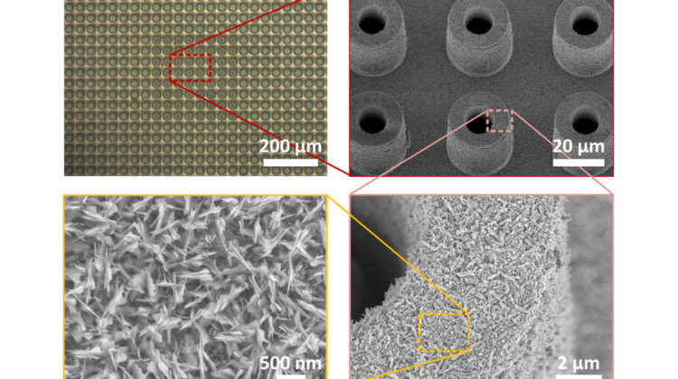
Adding a series of micro-scale cavities, or dents, to a surface can control the way in which bubbles form on it, keeping them effectively pinned to the locations of the dents and preventing them from spreading out into a heat-resisting film. In the present study, the researchers created an array of ten-micrometre-wide dents separated by about two millimetres to prevent film formation.
However, that separation also reduces the concentration of bubbles at the surface, which can reduce the boiling efficiency. To compensate for that, the team introduced a much smaller-scale surface treatment, creating tiny bumps and ridges at the nanometre scale, which increases the surface area and promotes the rate of evaporation under the bubbles.
Advertisement
The cavities were made in the centres of a series of pillars on the material’s surface. These pillars, combined with nanostructures, promote wicking of liquid from the base to their tops, and this enhances the boiling process by providing more surface area exposed to the water. In combination, the three ‘tiers’ of the surface texture – the cavity separation, the posts and the nano-scale texturing – provide a greatly enhanced efficiency for the boiling process.
‘Those micro-cavities define the position where bubbles come up,’ Song said. ‘But by separating those cavities by two millimetres, we separate the bubbles and minimise the coalescence of bubbles.’ At the same time, the nanostructures promote evaporation under the bubbles and the capillary action induced by the pillars supplies liquid to the bubble base. That maintains a layer of liquid water between the boiling surface and the bubbles of vapour, which enhances the maximum heat flux.
Although the team’s experiments have confirmed that the combination of these kinds of surface treatments can work and achieve the desired effects, the work was done under small-scale laboratory conditions that could not easily be scaled up to practical devices. ‘These kinds of structures we’re making are not meant to be scaled in its current form,’ said Ford Professor of Engineering Evelyn Wang, but rather were used to prove that such a system can work. One next step will be to find alternative ways of creating these kinds of surface textures so that these methods could more easily be scaled up to practical dimensions.
Advertisement
‘Showing that we can control the surface in this way to get enhancement is a first step,’ Wang said. ‘The next step is to think about more scalable approaches.’ For example, although the pillars on the surface in these experiments were created using clean-room methods commonly used to produce semiconductor chips, there are other, less demanding ways of creating such structures, such as electrodeposition. There are also a number of different ways to produce the surface nanostructure textures, some of which may be more easily scalable.
Among the potential applications for the process in its present form is the thermal management of electronic devices, an area that’s becoming more important as semiconductor devices get smaller and managing their heat output becomes ever more important. ‘There’s definitely a space there where this is really important,’ Wang said.
Advertisement
Even this application will take some time to develop because thermal management systems for electronics typically use liquids other than water, known as dielectric liquids. These liquids have different surface tension and other properties than water, so the dimensions of the surface features would have to be adjusted accordingly. Work on these differences is one of the next steps for the team’s ongoing research.
The research has been published in Advanced Materials.