
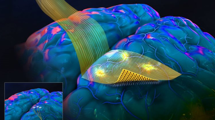
Engineering researchers from the University of California San Diego and Boston University have invented an advanced brain–computer interface that features a flexible and mouldable backing and penetrating microneedles. The flexible backing allows the device to more evenly conform to the brain’s complex curved surface and to more uniformly distribute the microneedles that pierce the cortex.
At present, the novel brain–computer interface has only been tested in rodents.The results so far suggest that its performance is on par with and even outperforms the so-called Utah Array, which is the existing gold standard for brain–computer interfaces with penetrating microneedles. The Utah Array has been demonstrated to help stroke victims and people with spinal cord injury. People who have had a Utah Array implanted can use their thoughts to control robotic limbs and other devices.
Advertisement

Unlike the Utah Array, which has a hard, inflexible backing, the backing of the new brain-computer interface is flexible, conformable and reconfigurable, which favours closer contact between the brain and the electrodes, allowing for improved and more uniform recording of the brain-activity signals.
In addition, the manufacturing technique used to produce soft-backed interface allows for larger sensing surfaces, so a significantly larger area of the brain surface can be monitored.The researchers built a device with 1,024 microneedles, which represents ten times more microneedles and ten times the area of brain coverage compared to existing technologies.
Advertisement

The new interface is also thinner and lighter than those that use traditional glass backings and the researchers say that the light, flexible backing may reduce irritation of the brain tissue that is in contact with the sensor array.
The flexible backings are also transparent, which the researchers may enable neuroscientists to perform fundamental research involving animal models that wouldn’t be possible otherwise. For example, the team demonstrated simultaneous electrical recording from arrays of penetrating micro-needles as well as optogenetic photostimulation.
Advertisement
The new interface’s properties are all by-products of the double-sided lithography approach that the researchers used.
The team’s manufacturing process allows them to build microscopic circuits and devices on both sides of a rigid silicon wafer. A flexible, transparent film is added to one side. Within this film, a bilayer of titanium and gold traces is embedded so that the traces line up with where the needles will be manufactured on the other side of the silicon wafer.
Working from the other side, the silicon is mostly etched away. What remains is a series of free-standing, thin, pointed columns of silicon – the microneedles. Their bases align with the titanium–gold traces within the flexible layer, which is also left behind after the silicon has been etched away. These titanium–gold traces are patterned via standard and scalable microfabrication techniques, allowing scalable production with minimal manual labour. The manufacturing process offers the possibility of flexible array design and scalability to tens of thousands of microneedles.
Advertisement
Details of the research have been published in Advanced Functional Materials.