
Researchers from the University of Glasgow’s James Watt School of Engineering have developed a new method of interfacial imprinting ultra-thin nanowires onto bendable, transparent polymeric substrates. This breakthrough development in nanofabrication could help support the development of new wireless, flexible, high-performance transparent electronic devices.
The technique, developed at the University’s meLAB and led by researcher Jungang Zhang, works by pairing laser engineering with a technique that uses electric fields to precisely arrange nanoscale materials, and could easily be scaled up to enable manufacture without the need to use cleanroom facilities.
Advertisement

The flexible materials created by the process are remarkably resistant to the electromagnetic interference caused by the increasingly ubiquitous presence of wireless signals in everyday life. While modern technology relies on 5G and wifi signals, they can cause problems with the sensitive electronics in vital equipment such as medical devices.
In the future, the team’s development could help pave the way for next-generation devices for use in wearable or implantable healthcare monitoring that combine outstanding performance with full shielding from unwanted signals.
Advertisement

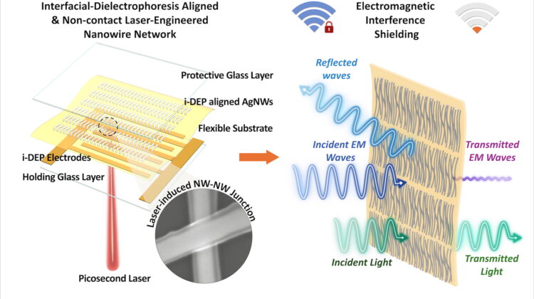
First, they use a non-uniform electric field to align silver nanowires a thousand times thinner than a human hair directly on a thin, flexible, transparent polyimide film. This process, called interfacial-dielectrophoresis or i-DEP, enables them to create very precise patterns including twists and turns in any direction. The team was able to precisely form the letters ‘NANO’ and ‘UOG’ on the polymer substrate using the i-DEP technique.
The i-DEP-aligned nanowires network with structural nanogaps are key to the material’s resistance to interference. The gaps act as capacitors, reducing the ability of external signals to affect internal electronics and creating what the team call a ‘capacitively coupled interwire network’.
Advertisement
In the second stage of the team’s manufacturing process, the nanowires are exposed to ultrafast pulses of picosecond laser light, which bonds junctions between the nanowires together to enable electrical interconnections. The process also strips the nanowires’ coating of insulating material, increasing their optical transparency by up to 10 per cent and reducing their electrical resistance by a factor of 46.
The team’s lab tests of their material demonstrated its remarkable ability to both shield against interference and maintain its transparency. The prototype films the team fabricated achieved more than 35 decibels of shielding effectiveness across the 2.2–6 GHz frequency band, enabling the blocking of more than 99.97 per cent of incident electromagnetic radiation. They also maintained 83 per cent optical transparency.
‘With this research, we’ve managed to open up a new design route that overcomes longstanding challenges in the field of nanotechnology by tapping in to the university’s expertise in microelectronics and soft material engineering, said Professor Hadi Heidari of the University of Glasgow’s Microelectronics Lab. ‘The electromagnetic interference shielding performance of the materials we created using this technique improves on the performance of non-aligned nanowires by more than 1,000 times for the first time. That improvement could enable the creation of a wide range of future flexible and implantable devices.’
Advertisement
The team’s technique also addresses key manufacturing challenges. Unlike conventional cleanroom fabrication, which is often limited to small wafer sizes and requires expensive, time-consuming processes, their relatively accessible approach is capable of producing larger materials. The researchers have demonstrated devices measuring 40 centimetres by 80 centimetres, which they say could be easily scaled up in future developments.
‘This is the first time anyone has overcome the longstanding trade-off between electrical conductivity and optical transparency in metallic nanowire networks. After our laser post-treatment, both the conductivity and transparency improve simultaneously,’ said Jungang Zhang, a research associate at the James Watt School of Engineering. ‘For flexible displays, wearable devices and implantable medical technologies, this shielding capability, paired with a high degree of transparency, is crucial. It ensures high-purity signal transfer for real-time healthcare monitoring while blocking unwanted electromagnetic noise. With a total thickness of just 5.1 micrometres, these films are incredibly thin yet highly effective, and we’re keen to explore and expand their potential in future research work.’
Advertisement
The research has been published in ACS Nano.