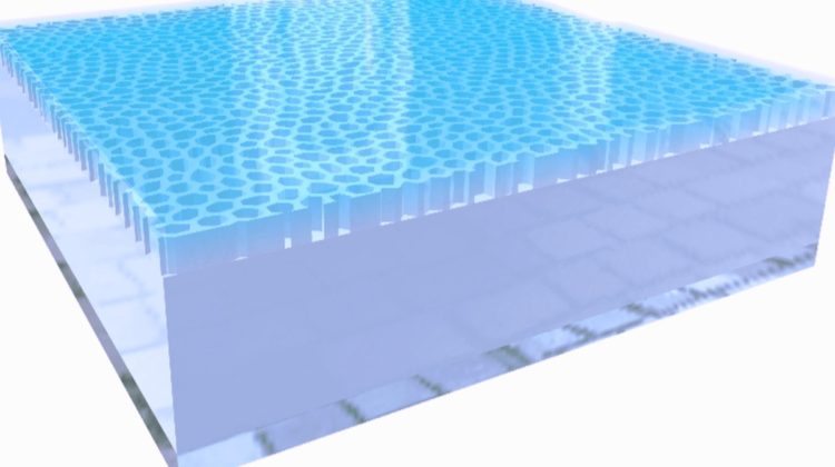
A team of scientists from the University of Surrey, Imperial College London and AMOLF in Amsterdam has used a light-trapping disordered honeycomb layer to increase the amount energy absorbed by wafer-thin photovoltaic panels by a quarter.
The team used the characteristics of sunlight, as well as insights from the design of butterfly wings and bird eyes, to design the honeycomb layer, which lies atop a wafer of silicon. The honeycomb design enables light absorption from any angle and traps light within the solar cell, enabling more energy to be generated.
‘One of the challenges of working with silicon is that nearly a third of light bounces straight off it without being absorbed and the energy harnessed, said Marian Florescu from the University of Surrey’s Advanced Technology Institute (ATI). ‘A textured layer across the silicon helps tackle this and our disordered, yet hyperuniform, honeycomb design is particularly successful.’
In the laboratory, the team achieved absorption rates of 26.3 mA per square centimetre, a 25 per cent increase on the previous record, achieved in 2017. The one-micrometre-thick photovoltaic cell had an efficiency of 21 per cent but the team anticipates that further improvements will push that figure higher, resulting in efficiencies that are significantly better than many commercially available photovoltaics.
‘There’s enormous potential for using ultra-thin photovoltaics,’ Florescu said. ‘For example, given how light they are, they will be particularly useful in space and could make new extra-terrestrial projects viable. Since they use so much less silicon, we are hoping that there will be cost savings here on Earth as well. There could also be potential to bring more benefits from the Internet of Things and to create zero-energy buildings powered locally.’
The new technology could also potentially benefit industries in which light management and surface engineering are crucial, such as photo-electrochemistry, solid-state light emission and photodetectors.
The team is now looking for commercial partners and developing manufacturing techniques.
The research has been published in Photonics.


