
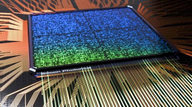
Most of the world’s internet traffic spends at least part of its journey travelling through optical fibre. It’s fast, efficient and remarkably good at carrying light over long distances with very little signal loss. Shrinking that same performance onto a silicon chip, however, has proved far more difficult.
Researchers at the California Institute of Technology (Caltech) now believe they’ve taken a significant step towards solving that problem.
The team has developed a way to fabricate photonic integrated circuits (PICs) using the same type of glass found in optical fibre, achieving exceptionally low optical losses at visible wavelengths. Reported in Nature, the approach could improve a wide range of technologies that rely on guiding light across miniature circuits, from optical clocks and precision sensors to AI data centres and quantum computing.
Unlike conventional electronic chips, which move information using electrical signals, photonic chips use light. That offers several advantages, including higher bandwidth and lower energy consumption. The challenge is keeping that light confined within microscopic waveguides without losing energy as it travels.
Advertisement

Traditional photonic circuits often rely on silicon nitride, but performance tends to suffer at visible wavelengths because tiny imperfections along the waveguide scatter light. Even minute surface roughness can significantly reduce efficiency.
The Caltech team tackled the problem by switching to germano-silicate glass, the same material widely used to manufacture optical fibre. Because the material melts at a comparatively low temperature, the researchers were able to heat the completed waveguides in a furnace, allowing the surface to reflow until it became smooth at almost the atomic level.
That reduction in surface roughness dramatically cuts scattering losses. According to the researchers, the new platform outperforms previous silicon nitride devices by around a factor of 20 at visible wavelengths, while also matching state-of-the-art performance in the near-infrared.
Rather than laying the waveguides out in straight lines, the team also wound them into tight spirals. The arrangement allows light to travel much greater effective distances while occupying only a few square centimetres of chip area, much like winding kilometres of optical fibre onto a spool.
At first glance, measuring losses over distances of metres or even kilometres might seem unnecessary for a chip that fits comfortably in the palm of a hand. In practice, though, many photonic devices depend on light circulating repeatedly through tiny ring resonators. The longer the light can remain trapped without losing energy, the better those devices perform.
Advertisement
That has important consequences for applications where precision matters. Lasers built using the new platform showed more than a hundredfold improvement in coherence compared with previous designs, potentially benefiting optical clocks, gyroscopes, atomic sensors and ion-trap quantum systems. The researchers also point to lower-energy optical links for AI data centres, where reducing losses could help cut the power required to move growing volumes of information between processors.
The work is still at a relatively early stage, but it highlights a broader trend in photonics. As computing demands continue to grow, engineers are increasingly looking beyond conventional electronics and towards optical systems capable of carrying more information with less energy. Bringing fibre-like performance onto standard silicon wafers could prove to be one of the key enabling technologies.